Wide-bandgap semiconductors

– the hidden champions of green energy

Less loss, less cooling, smaller devices

Modern power semiconductors are based on special wafer materials (silicon carbide or gallium nitride) and have specific properties optimizing energy efficiency.

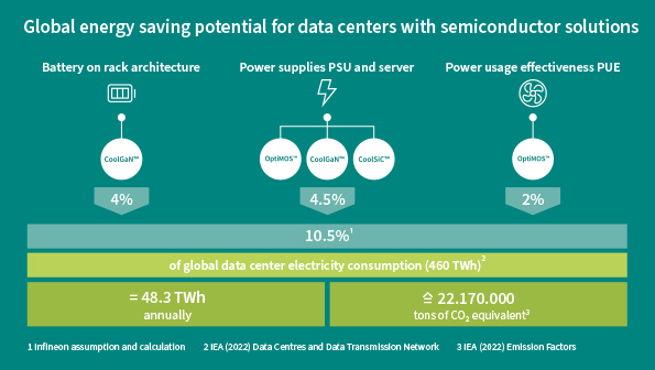
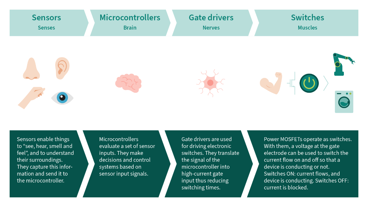
For the refrigerator to cool at home, for the assembly lines to run in a factory, for the photovoltaic system to produce solar power, or for digital data to be reliably processed in a data center: Different types of collaborating semiconductors are necessary to process electricity in electronic applications in all areas of life. Sensors, microcontrollers, gate drivers and power devices are the key ingredients in applications running on electricity. They make sure that energy is converted in an efficient, reliable, smart and secured way.

New technologies have been available for several years in the field of power devices, referred to as wide-bandgap semiconductors: Silicon carbide and gallium nitride. They have many advantages in terms of energy efficiency and thus make an important contribution to decarbonization. Their structure and properties let them handle higher voltages and frequencies and still function smoothly at higher temperatures.

Gallium Nitride (GaN)

What is GaN?

Gallium nitride semiconductors are compound semiconductors, made from Gallium (Ga) and Nitride (N).

Wafers made solely from GaN would be too costly to produce. Here manufacturers have a trick up their sleeve: They use silicon wafers – and apply an ultra-thin layer of gallium nitride. This highly complex metal-organic chemical gas deposition takes place at Infineon in special reactors: Here silicon wafers are exposed to various vaporized chemicals at a temperature of 1200 degrees Celsius. In a complex chemical reaction, the GaN layer, which is only a few thousandths of a millimeter thick, is created from the gaseous materials in several hours.

The electronic circuits are then attached to this layer. Due to the special arrangement of the gallium nitride on the silicon base material, the current in the chips runs parallel to the surface, whereas with SiC it runs through the chip. Although this means that GaN chips cannot process quite as high voltages, they can on the other hand switch extremely quickly with almost no loss.

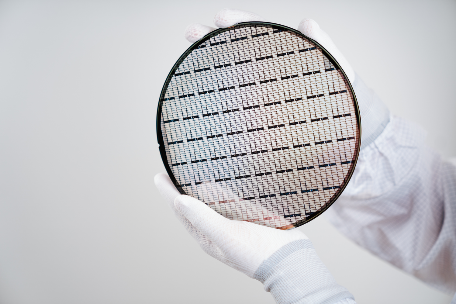
Infineon pioneers world’s first 300mm power gallium nitride (GaN) technology

Infineon has achieved a major milestone by developing the world's first 300mm power gallium nitride (GaN) wafer technology. As the first company to master this groundbreaking technology in a high-volume manufacturing environment, Infineon is poised to significantly drive the market for GaN-based power semiconductors.

The shift to 300mm wafers offers several advantages over the traditional 200mm wafers, including a 2.3-fold increase in chip production per wafer. Moreover, the 300mm GaN technology can leverage existing 300mm silicon manufacturing equipment, as the production processes for gallium nitride and silicon are very similar. This allows Infineon to pilot reliable GaN technology on its existing high-volume silicon 300mm production lines, enabling accelerated implementation and efficient use of capital. Once fully scaled, 300mm GaN production is expected to achieve cost parity with silicon on the RDS(on) level, making GaN products comparable in cost to their silicon counterparts. 300mm GaN is another milestone in Infineon’s strategic innovation leadership and supports the mission of decarbonization and digitalization.

What are the benefits of GaN?

Gallium nitride transistors are key in designing smaller and more efficient power solutions. Technically speaking, they enable higher switching frequencies while keeping loss at very low levels.

This way, GaN technology significantly contributes to reducing system costs and complexity thanks to the need for fewer capacitors, smaller inductors and smaller heat sinks.

Today this innovative technology is already part of many applications and devices in our daily lives, such as USB-C adapters and chargers, EV chargers, solar inverters, telecom rectifiers and server power supplies. The advantages are of great importance to many users: longer battery life, faster charging and enhanced data communication capabilities.

In short, GaN components improve power density, efficiency and reliability.

GaN in everyday applications - Examples

GaN in data centers - cool down and think small


With changing lifestyles, digitalization and the ongoing push for artificial intelligence, data volumes are also growing exponentially. At the same time, we see energy consumption in data centers strongly increasing. According to the IEA, in 2022 data centers consumed around 2% of the world's total electricity (= 460 TWh). The key questions are: Where is energy needed, for what and how can demand be reduced?

Did you know that data centers use up to 50% of their energy for cooling and backup power alone? There is a great need for alternative energy solutions. In addition to established semiconductors, in particular new wide-bandgap technologies like silicon carbide (SiC) and gallium nitride (GaN) play a crucial role. GaN technology alone has a global savings potential of 21 TWh annually. Looking at the impact of all Infineon technologies together (Si, SiC, GaN), we could potentially save the incredible amount of 48 TWh.

What are the benefits of GaN in data centers?


GaN transistors (HEMTs) allow us to push the frontiers for both energy efficiency and space. Technically speaking, they pave the way for up to 98.5 percent efficiency in 48 V servers and a power density of up to 100 W/inch3 for 12 V servers. CoolGaN™ transistors increase switching frequencies by a factor of 10 and reduce energy loss by up to 50% in any given power supply.

As a result, data centers can handle more power in the same or less space and need less cooling energy. For data center operators this means significant savings on operational expenditures and capital expenditures. And this means a huge savings potential on CO2 emissions for our environment.

GaN for chargers and adapters - smaller size, more power, less e-waste


Today's chargers for communication devices need to be small, powerful, and reliable. Not to mention green! But what about energy lost during voltage conversion? How can these losses be avoided? The secret lies in getting the semiconductor technology right.

Just imagine: If every smartphone charger worldwide used Infineon power components, we would save the electricity consumed every year by all homes in a big city like Munich. In other words, we could save around 2.3 GWh, which corresponds to more than 1000 tons of CO2 equivalent!

The great potential of gallium nitride


  1. State-of-the-art microelectronics inside chargers and adapters can reduce waste heat. The semiconductor technology gallium nitride (GaN) is particularly effective. GaN transistor components enable a higher switching frequency in the voltage converter while keeping loss at very low levels. In simple terms, GaN semiconductors translate into significant electrical energy savings in chargers.
  2. In addition, GaN technology enables higher power densities. Devices become smaller without compromising on performance or charging time.
  3. Finally, GaN power stages and transistors are driving the USB-C standard. It is expected that USB-C will save 11,000 tons of e-waste every year.


Get deeper insights into Infineon's GaN portfolio here

Silicon Carbide (SiC)

What is SiC?

Silicon carbide semiconductors are compound semiconductors made of Silicon (Si) and Carbon (C). Compared to "traditional" silicon, the production of SiC is highly complex.

Although SiC occurs naturally as carborundum, it is too impure in nature, so the crystals have to be grown, just like silicon. While silicon crystals grow to a meter long within two days at around 1500 degrees, silicon carbide needs up to two weeks at 2400 degrees to grow a raw crystal, called a puck, that is at most ten centimeters long. In the next step, fine diamond wires are used to cut this puck into extremely thin wafers. About half of the material is lost during sawing and grinding.

But there is a solution: Infineon works with a separation technology called "Cold Split". A laser creates a "defect layer" onto which a polymer is applied. During cooling, the semiconductor and the polymer connected to it expand differently. This causes mechanical stress that splits the wafer. The process has been around for a while, but it only became commercially attractive with silicon carbide. 

Silicon carbide wafers are more expensive than silicon wafers and are extremely thin. However, with the same performance, SiC chips are smaller than Si components by a factor of 5. Therefore, the power handling capability gained per wafer is much bigger.

Globally, there is extensive research relating to SiC. The EU for example is supporting the "European SiC Value Chain for a greener economy" with 89 million euros. And for a good reason: The market is strongly growing to 6.3 billion dollars by 2027 according to the consultancy agency Yole. And SiC has unique advantages for certain industries.

What are the benefits of SiC?

Electric cars, trains and industrial drives consume less electricity, solar modules can feed more power to the grid thanks to a single material: silicon carbide. This semiconductor material unfolds its potential wherever direct and alternating current are converted – between PV modules and the power grid, between batteries and electric motors and between the grid and home storage systems. Considerable amounts of electricity flow in these processes. Energy is usually lost with each power conversion. This can be reduced by SiC – to a high extent. Depending on the area of application, experts see a potential 30 percent loss reduction. That quickly adds up to several megawatt-hours of savings.

The secret of silicon carbide is its wide bandgap. This means that silicon carbide can withstand higher internal electric fields than silicon can, allowing the use of thinner semiconductor layers with lower resistance and correspondingly less power loss. And because of its rigid crystal structure, silicon carbide also withstands higher temperatures and dissipates heat better. Both factors can significantly reduce cooling efforts, leading to massive CO2 savings potential.

In addition, silicon carbide enables higher switching frequencies. The advantages of this can be seen in inverters. These components "chop" the direct current into many small portions and reassemble them as alternating current. And the higher the switching frequency, the smaller the respective current portions and the smaller the passive components required.

SiC in everyday applications – Examples

SiC for solar inverters - smaller size, more power


A prominent example where SiC has made significant design miniaturization possible is solar inverters. 

While a 100-kilowatt inverter for a photovoltaic system weighed more than a ton in 2008, modern 125 kW units weigh well under 100 kilograms. Such systems, with an efficiency of up to 99 percent, have already been on the market for a few years.

The special material properties of SiC are ideal: They allow for higher currents than traditional silicon semiconductors of the same chip size with significantly reduced loss. By enabling higher switching frequencies, SiC semiconductors help to massively reduce the size and weight of passive components such as inductors. This enables more compact PV inverters and helps lower system costs. 

In short, Infineon's SiC components help improve the overall efficiency of a solar power plant.

SiC for electric vehicles - greater range, smaller battery, faster charging


Silicon carbide in electric vehicles enables more efficiency, higher power density and better performance. In particular with an 800 V battery system and a large battery capacity, silicon carbide leads to higher efficiency in inverters and thus enables longer ranges and lower battery costs. SiC furthermore improves the efficiency and power density of the on-board charger. The material enables bi-directional power flow, from the grid to the battery and vice versa. SiC also has a positive impact on battery management: It enables greater vehicle range with the same battery size, or smaller and lighter batteries with the same range.

In addition, charging with the respective infrastructure can be much faster thanks to SiC. Thinking further, power semiconductors foster sustainability: Highly efficient vehicles have lower weight due to optimized battery capacity, less cooling effort and optimized wire harnesses. This enables a sustainable circular lifecycle and reduces raw materials consumption. 

In short, Infineon's SiC system solutions help improve the overall efficiency of the vehicle – especially in the drive train, the traction inverter and the on-board charger. 


Get deeper insights into Infineon’s SiC portfolio here

Explore how to increase energy efficiency in other use cases