The split gate trench concept has revolutionized the field of power MOSFETs
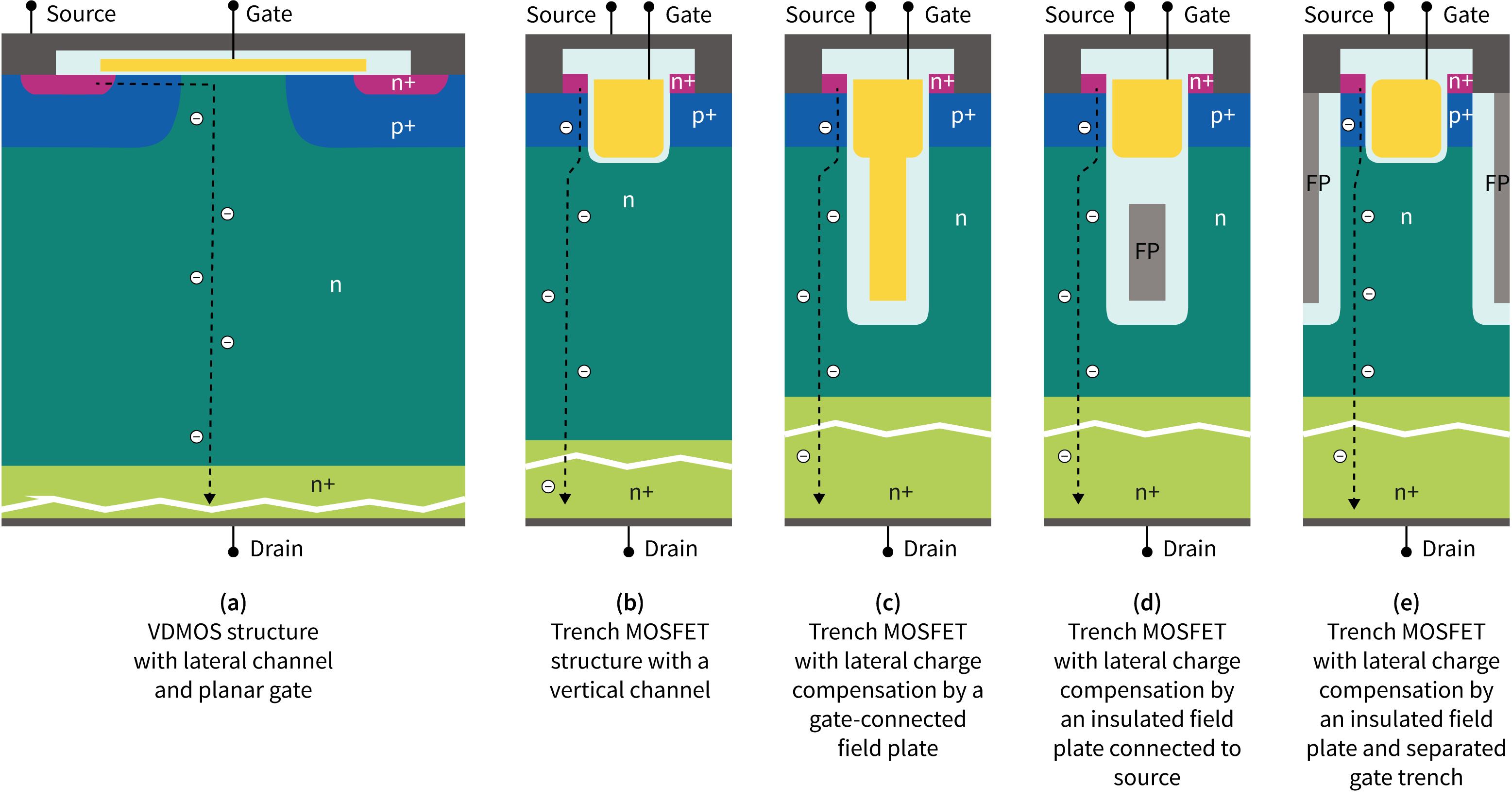
MOSFET technology has been widely recognized as an excellent option for switches in power management circuits since its introduction. Commercially available since the late 1970s, vertical diffused MOSFET (VDMOS) structures were the first to fulfill the need for a power switch, as illustrated in the picture below on the left (Figure 1a).
It took more than a decade of device design and process engineering progress to overcome the limitation of the high on-state resistance that restricted the current-handling capabilities of the VDMOS. This finally led to the commercialization of the first trench-gate MOSFETs (Figure 1b). By moving the channel in the vertical direction, this device concept enables a reduction in cell pitch without negatively affecting current spreading. A new era started with the introduction of charge-compensated structures, exploiting the same principle as superjunction devices. Introducing devices that use an insulated deep field plate as an extension of the gate electrode enabled the lateral depletion of the drift region in the off state (Figure 1c).
As the transfer capacitance reduces abruptly when the mesa region is fully depleted, a field plate was introduced to overcome this challenge. This field plate is electrically connected to the source potential and isolated from the gate electrode (Figure 1d).
To reach the next level in power MOSFET evolution, new MOSFET devices are required to provide improvements across all Figure Of Merits. This is needed to enable high-frequency SMPS operation, whereby losses are associated with charges (switching) and on-state resistance (conduction). To meet these more demanding requirements, a novel cell structure has been developed, pioneering true three-dimensional charge compensation for the first time.
For further details of Infineon's innovative approach to elevate power MOSFET design to new heights, you can find more details found here.