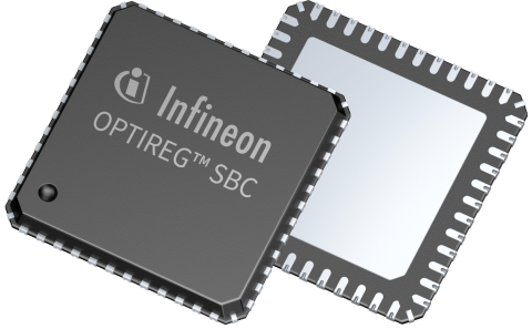
TLE9262BQX V33
The TLE9262BQXV33 is a monolithic integrated circuit in an exposed pad VQFN-48 (7mm x 7mm) power package with Lead Tip Inspection (LTI) feature to support Automatic Optical Inspection (AOI). The device is designed for various CAN-LIN automotive applications as main supply for the microcontroller and as interface for a LIN and CAN bus network. To support these applications, the System Basis Chip (SBC) provides the main functions, such as a 3.3V lowdropout voltage regulator (LDO) for e.g. a microcontroller supply, another 5V low-dropout voltage regulator with off-board protection for e.g. sensor supply, another 3.3V/1.8V regulator to drive an external PNP transistor, which can be used as an independent supply for off-board usage or in load sharing configuration with the main regulator VCC1, a HS-CAN transceiver supporting CAN FD and LIN transceiver for data transmission, high-side switches with embedded protective functions and a 16-bit Serial Peripheral Interface (SPI) to control and monitor the device. Also implemented are a configurable timeout / window watchdog circuit with a reset feature, three Fail Outputs and an undervoltage reset feature. The device offers low-power modes in order to minimize current consumption on applications that are connected permanently to the battery. A wake-up from the low-power mode is possible via a message on the buses, via the bi-level sensitive monitoring/wake-up inputs as well as via cyclic wake. The device is designed to withstand the severe conditions of automotive applications.
特長
- Very low quiescent current consumption in Stop- and Sleep Mode
- Periodic Cyclic Wake in SBC Normal- and Stop Mode
- Periodic Cyclic Sense in SBC Normal-, Stop- and Sleep Mode
- Low-Drop Voltage Regulator 3.3V, 250mA
- Low-Drop Voltage Regulator 5V, 100mA, protected features for off-board usage
- Low-Drop Voltage Regulator, driving an external PNP transistor - 3.3V in load sharing configuration or 3.3V/1.8V in stand-alone configuration, protected features for off-board usage. Current limitation by shunt resistor (up to 350mA with 470mΩ external shunt resistor) in stand-alone configuration
- High-Speed CAN Transceiver:
– fully compliant to HS-CAN standard ISO 11898-2:2016
– supporting CAN FD communication up to 5 Mbps - LIN Transceiver LIN 2.2a, J2602 with configurable TXD timeout feature and LIN Flash Mode
- Fully compliant to “Hardware Requirements for LIN, CAN and FlexRay Interfaces in Automotive Applications” Revision 1.3, 2012-05-04
- Four High-Side Outputs 7Ω typ.
- Dedicated supply pin for High-Side Outputs
- Two General Purpose High-Voltage In- and Outputs (GPIOs) configurable as add. Fail Outputs, Wake Inputs, Low-Side switches or High-Side switches
- Three universal High-Voltage Wake Inputs for voltage level monitoring
- Alternate High-Voltage Measurement Function, e.g. for battery voltage sensing
- Configurable wake-up sources
- Reset Output
- Configurable timeout and window watchdog
- Up to three Fail Outputs (depending on configuration)
- Overtemperature and short circuit protection feature
- Wide supply input voltage and temperature range
- Software compatible to all SBC families TLE926x and TLE927x
- Green Product (RoHS compliant) & AEC Qualified
- PG-VQFN-48 leadless exposed-pad power package with Lead Tip Inspection (LTI) feature to support Automatic Optical Inspection (AOI)


