Infineon pioneers world’s first 300 mm power gallium nitride (GaN) technology – an industry game-changer
- Infineon will shape the rapidly growing GaN market with this groundbreaking GaN 300 mm technology
- Infineon leverages existing large scale 300 mm silicon manufacturing to maximize capital efficiency in GaN production
- 300 mm GaN will help achieve cost parity with silicon over time
Munich, Germany and Villach, Austria – 11 September 2024 – Infineon Technologies AG (FSE: IFX / OTCQX: IFNNY) today announced that the company has succeeded in developing the world’s first 300 mm power gallium nitride (GaN) wafer technology. Infineon is the first company in the world to master this groundbreaking technology in an existing and scalable high-volume manufacturing environment. The breakthrough will help substantially drive the market for GaN-based power semiconductors. Chip production on 300 mm wafers is technologically more advanced and significantly more efficient compared to 200 mm wafers, since the bigger wafer diameter offers 2.3 times more chips per wafer.
GaN-based power semiconductors find fast adoption in industrial, automotive, and consumer, computing & communication applications, including power supplies for AI systems, solar inverters, chargers and adapters, and motor-control systems. State-of-the art GaN manufacturing processes lead to improved device performance resulting in benefits in end customers’ applications as it enables efficiency performance, smaller size, lighter weight, and lower overall cost. Furthermore, 300 mm manufacturing ensures superior customer supply stability through scalability.
“This remarkable success is the result of our innovative strength and the dedicated work of our global team to demonstrate our position as the innovation leader in GaN and power systems,” said Jochen Hanebeck, CEO of Infineon Technologies AG. “The technological breakthrough will be an industry game-changer and enable us to unlock the full potential of gallium nitride. Nearly one year after the acquisition of GaN Systems, we are demonstrating again that we are determined to be a leader in the fast-growing GaN market. As a leader in power systems, Infineon is mastering all three relevant materials: silicon, silicon carbide and gallium nitride.”
Infineon has succeeded in manufacturing 300 mm GaN wafers on an integrated pilot line in existing 300 mm silicon production in its power fab in Villach (Austria). The company is leveraging well-established competence in the existing production of 300 mm silicon and 200 mm GaN. Infineon will further scale GaN capacity aligned with market needs. 300 mm GaN manufacturing will put Infineon in a position to shape the growing GaN market which is estimated to reach several billion US-Dollars by the end of the decade.
This pioneering technological success underlines Infineon's position as a global semiconductor leader in power systems and IoT. Infineon is implementing 300 mm GaN to strengthen existing and enabling new solutions and application fields with an increasingly cost-effective value proposition and the ability to address the full range of customer systems. Infineon will present the first 300 mm GaN wafers to the public at the electronica trade show in November 2024 in Munich.
A significant advantage of 300 mm GaN technology is that it can utilize existing 300 mm silicon manufacturing equipment, since gallium nitride and silicon are very similar in manufacturing processes. Infineon’s existing high-volume silicon 300 mm production lines are ideal to pilot reliable GaN technology, allowing accelerated implementation and efficient use of capital. Fully scaled 300 mm GaN production will contribute to GaN cost parity with silicon on R DS(on) level, which means cost parity for comparable Si and GaN products.
300 mm GaN is another milestone in Infineon’s strategic innovation leadership and supports Infineon’s mission of decarbonization and digitalization.
About Infineon
Infineon Technologies AG is a global semiconductor leader in power systems and IoT. Infineon drives decarbonization and digitalization with its products and solutions. The company has around 58,600 employees worldwide and generated revenue of about €16.3 billion in the 2023 fiscal year (ending 30 September). Infineon is listed on the Frankfurt Stock Exchange (ticker symbol: IFX) and in the USA on the OTCQX International over-the-counter market (ticker symbol: IFNNY).
Further information is available at www.infineon.com
This press release is available online at www.infineon.com/press
About Infineon Austria
Infineon Technologies Austria AG is a subsidiary of Infineon Technologies AG, a global semiconductor leader in power systems and IoT. Semiconductors are essential for mastering the energy-related challenges of our time and helping to shape the digital transformation. Infineon's microelectronics drive decarbonization and digitalization and enable groundbreaking solutions for green and efficient energy, clean and safe mobility as well as a smart and secure IoT.
Infineon Austria pools competencies for research and development, production as well as global business responsibility. The head office is in Villach, with further branches in Graz, Klagenfurt, Linz, Innsbruck and Vienna. With 5,886 employees (including around 2,500 in research and development) from 79 nations, the company generated revenue of EUR 5.6 billion in the 2023 fiscal year (ending 30 September). With research expenditure of 672 million euros, Infineon Austria is one of the strongest research companies in Austria.
Press Photos
-
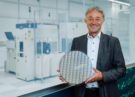 Thomas Reisinger, Chief Operations Officer Infineon Technologies Austria: "We are very proud to have reached a groundbreaking milestone with the development of the technology for the industrial production of the world’s first 300mm power gallium nitride wafers. Our Villach team has contributed significantly to the success of the Group in the field of power semiconductors, which is a key lever for decarbonization and digitalization. In recent years, major investments have been made in Villach as the global competence center for power electronics in the further development of gallium nitride and silicon carbide. With this world first, we have once again proven that innovation is in our DNA. We are constantly expanding our expertise and driving forward our innovation leadership as part of a global team."Thomas Reisinger_Infineon Austria_GaN 300 mm
JPG | 3.05 mb | 5160 x 3688 px
-
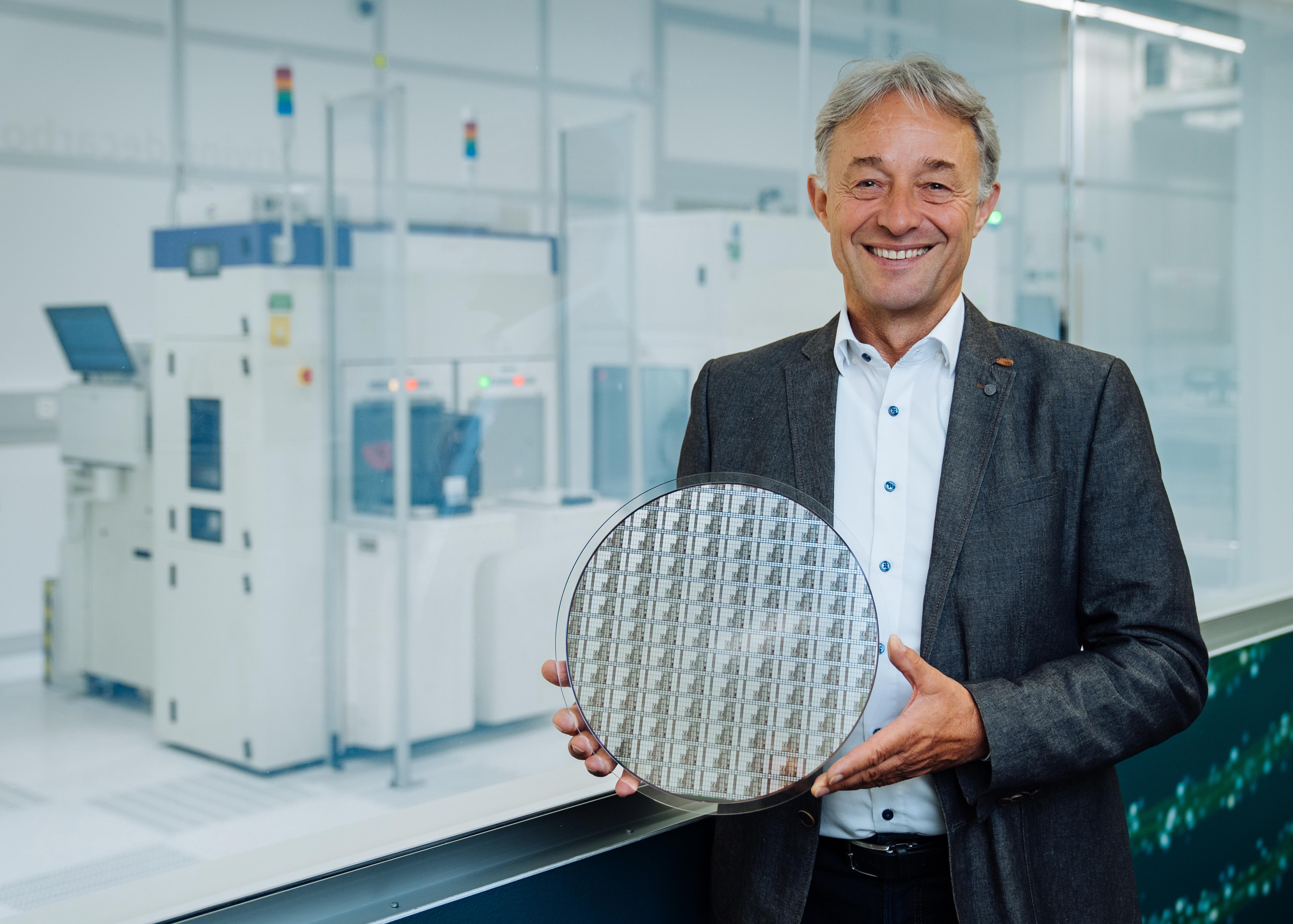
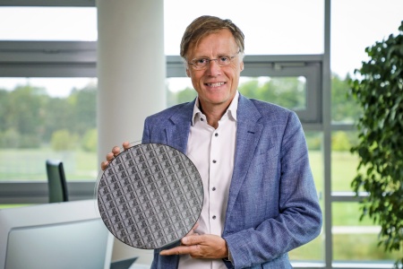 Infineon CEO Jochen Hanebeck holds one of the world’s first 300 mm GaN Power wafers produced in an existing and scalable high-volume manufacturing environment.Inf CEO Hanebeck_GaN300
JPG | 2.06 mb | 2126 x 1417 px
-
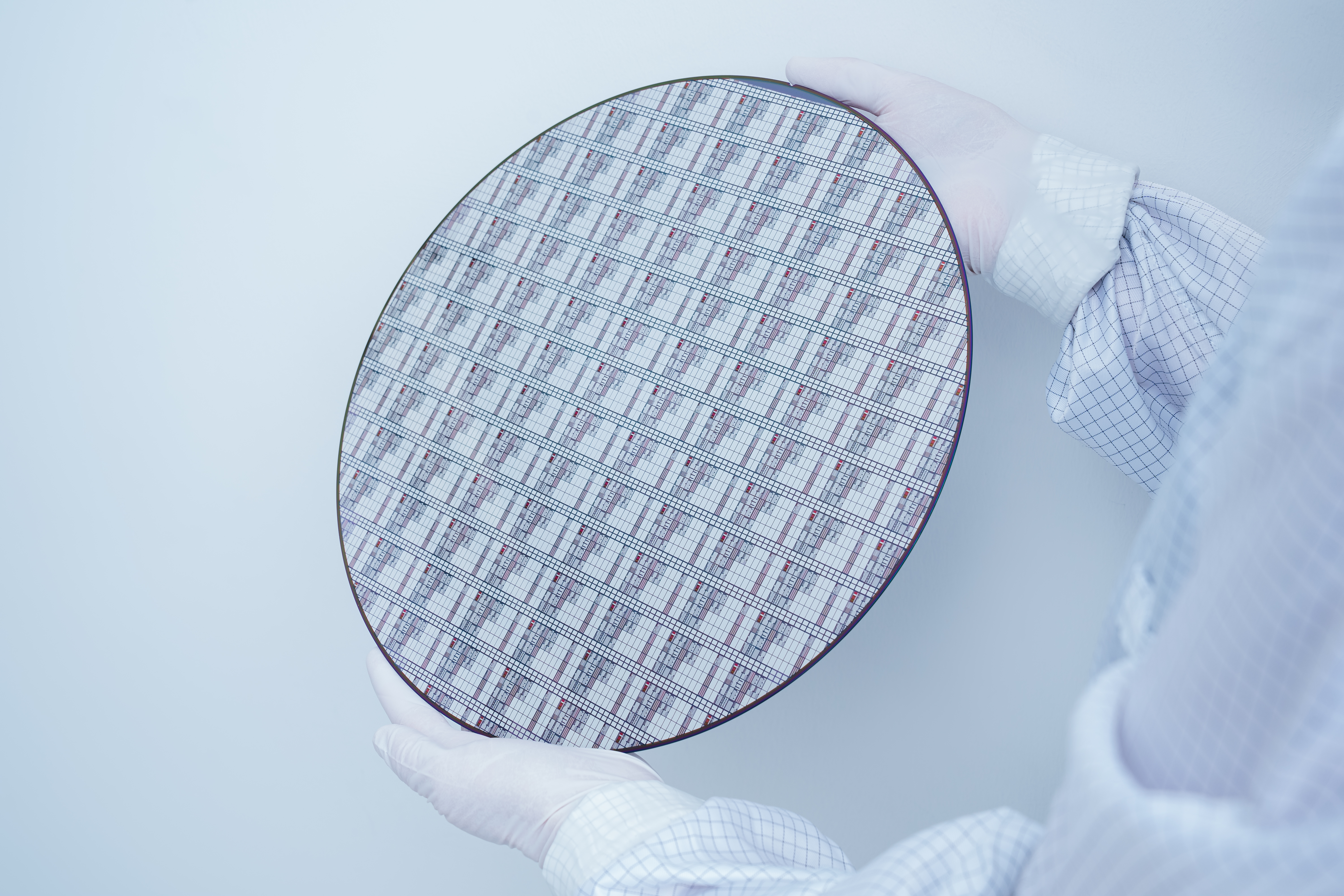
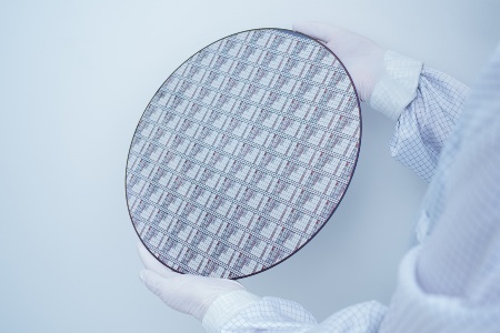 Chip production on 300 mm wafers is more efficient compared to 200 mm wafers, since the bigger wafer diameter offers 2.3 times more chips per wafer.Inf_GaN_Wafer-300
JPG | 9.87 mb | 6000 x 4000 px
-
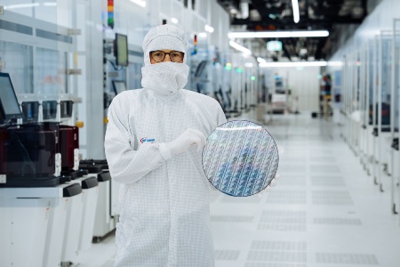 A technical engineer in the cleanroom at Infineon Technologies in Villach, Austria, holds a 300 mm gallium nitride wafer.Techniker im Reinraum mit GaN300-Wafer
JPG | 1.88 mb | 6000 x 4000 px